The T238+ is the successor to the T238. It assumes all the functions of the T238 and adds an MX-614-based modem as a daughter card to take over the basic TNC functions. This allows the T238+ to get on the air with only a radio, a TNC is no longer required.
The form factor of the T238+ has also been significantly reduced. It is now the same size as the LCD module and attaches directly to it. There is now a seperate button board that can be panel mounted.
The only significant feature that has been scaled back on the T238+ is the program development support. For program development a special crystal frequencys is required along with a debugger interface. For the T238+ you will need to supply your own crystal if you want to develop code. The single RS-232 header can be repurposed to become a debug header if needed as well. Instructions for how to do this are at the bottom of this page.
Since the T238+ is no longer available as a kit, gerbers for the boards are
available below if you would like to have a board built. Alternatively,
building a board with wire-wrapping or other methods works nicely too.
T238 Modem Assembly document
T238 Main board gerbers
Here are the documents:
T238+ Assembly document
T238+ Schematic
T238+ Board Layout
T238+ Operations Manual
T238 Modem schematic
T238 Modem Layout
T238 Modem board gerbers
T238 Button board gerbers
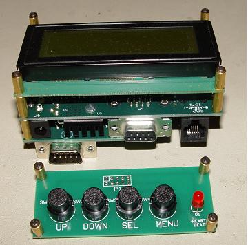
View of the assebled main unit (LCD, Main Board, and Modem) along with the
button board.
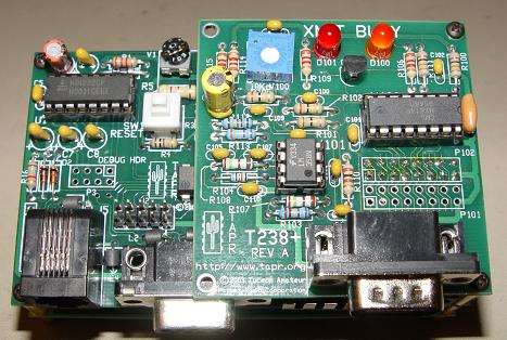
View of the back of the completed assembly, showing how the Modem board overlaps
the main board. Note that the potentiometer on this main board does not match
the one provided in the kit, the kit provided one looks like the one on the
Modem board. Also note, that the potentiometer provided does not match the
silkcreen outline. The small standoffs are on the opposite side indicated by
the silkscreen. Insert the potentiometer the way the leads indicate, not the
silkscreen.
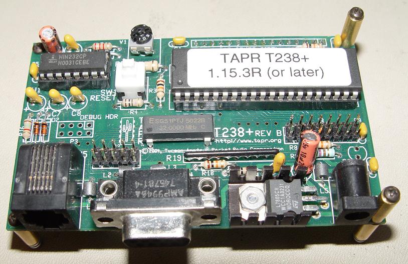
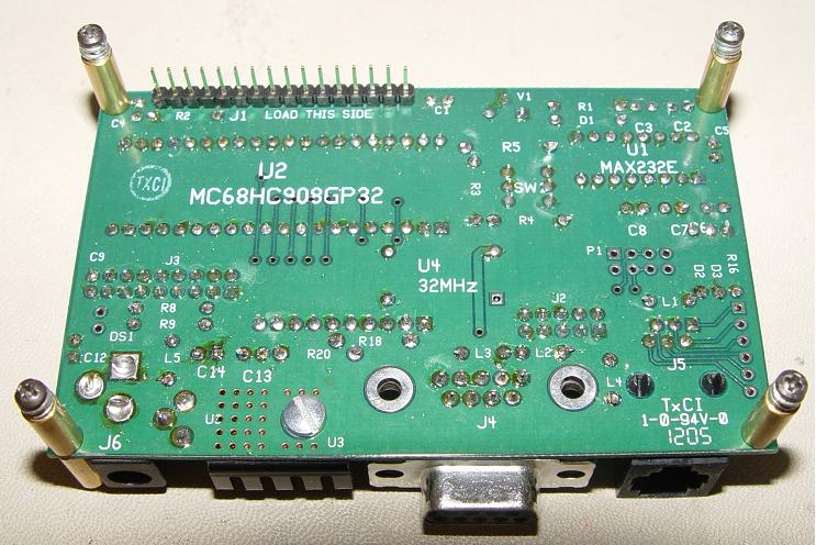
A complete view of the component side of the main board. Items to note are the
heat sink assembly and that J1 (for the LCD) is not visisble on this side as it
is soldered to the other side of the board.
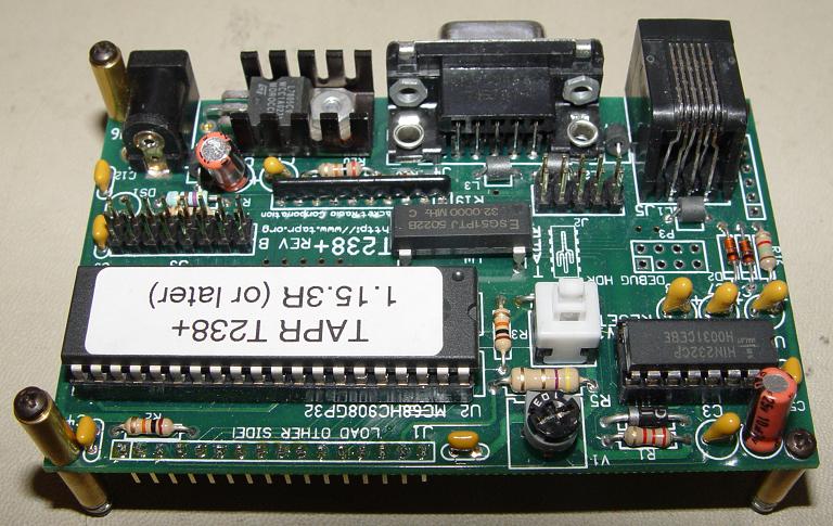
An opposite side view of the component side of the main board. This affords
another view of the heat sink assembly. Of particular note here is showing
the orientation of the reset switch. Note the hole in the plunger. It must
be oriented toward the potentiometer. J1 is visible on the opposite side of
the board. Finally note again that the potentiometer is not the one issued
with your kit.
Primary note here is J1's location.

Note that the provided potentiometer provided does not match the silkcreen
outline. The small standoffs are on the opposite side indicated by the
silkscreen. Insert the potentiometer the way the leads indicate, not the
silkscreen. Note also that P102 is mounted on the OTHER side of the board.
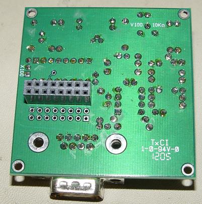
Not much to show here other than P102s mounting position.
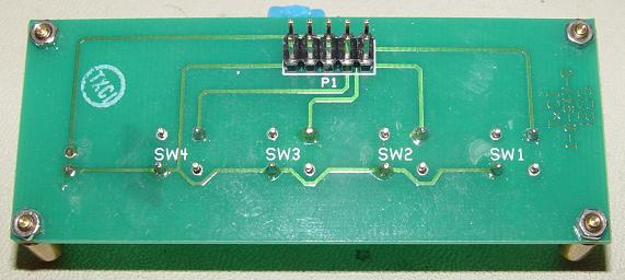
The back side of the button board contains only the connector. See the top
of these pictures for the front side view.
IMPORTANT! Before solding in J3, break the traces on the back side of the board between pins 3 and 5 and also pins 4 and 6. Carefully remove the oscillator (U4). Solder in J3 and the socket for U4.
Operational Mode:
J3, short pins 3/5, and 4/6
Install 32MHz crystal oscillator in U4
Debug Mode:
J3, short pins 1/3, 2/4, and 7/8
Install 9.8304MHz crystal oscillator in U4
In debug mode hook up your PCs serial interface to the T238+. Using the P&E toolset, you need to tell them you will be doing manual resets.